A Look at the 8-bit computer components.
Objectives
Notes
- Registers
- Page
- The video for this is here.
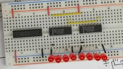
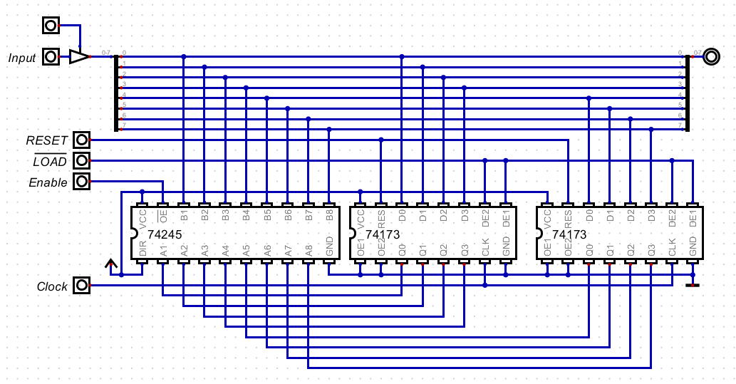
- The 74x173
- This is a 4 bit register.
- 4 data inputs(D), 4 data outputs (Q)
- M and N lines control output, both high = output
- G1 and G2 control input, both low = read data
- CLR clears the register
- Clock
- I think this chip is different from the data sheet, but matches Ben's diagrams.
- The 74x245 is a 8-bit tri state device.
- 16 data ports, 8 A, 8B
- A direction indicator (DIR) (0 B->A, 1 A->B)
- OE - output enable, low enables .
-
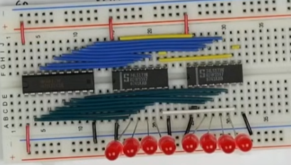
- Note he ties G1 and G2 (enable not ) of both chips together to ground (pins 1 and 2).
- He ties pins 9 and 10 (m and n, output control) together (yellow)
- He ties the clock together (7 white)
- The clear lines (15 yellow) are tied together as well.
- The direction pin (1) on the tristate chip is tied to positive.
- He then adds the wires connecting the chips
-
- Finally he adds
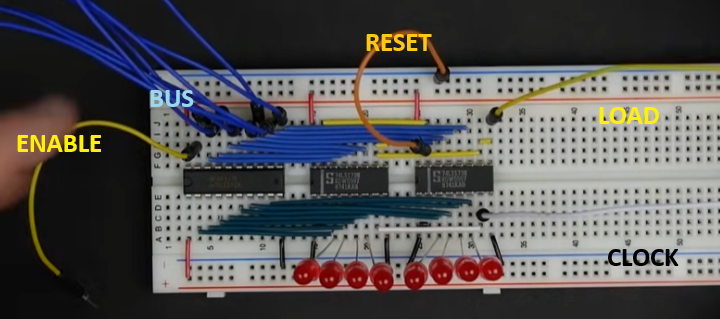
- 8 blue jumpers which he connects to the bus
- A yellow enable line (left side) - drives output from tri-state
- A yellow load line (left side)
- A white clock line (Right side)
- An orange reset line
-
- In the digital file
- The lines are not labeled the same
- I set enable and load to be 1 by default.
- My internal wires are the bus, but ...
-
- A Digital Version
- You can watch him test the registers here
- The b register is the same.
- The instruction register is a bit different.
- He loads it from the bus.
- But for output, he only sends the bottom 4 bits to the bus
- At about 4:43 on the above video he hooks up two registers and transfers data.
- He adds in the IR and at about 9:40 he executes a
load 11 instruction!