- Has n address bits to select among the2n data stored.
- It has a single m bit output, for the data that was selected
- It has an enable line
- Enter the address on the address line
- enable the chip via the enable line.
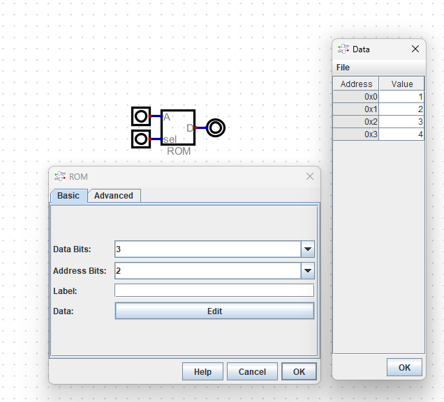
- Because it is simple.
- And I need it to do anything else.
- I have moved the tristate device outside of the register file
- This allows me to see what is coming out of this device.
- I have also added a second output.
- The idea is eventually to connect one output directly to the alu
- And the other to the bus
- We could implement an instruction like
add r0, r1- If we get to that point, all math will be between two registers
- Or between a register and an immediate.
-
add r0, immediate - This is an architecture decision that drives the organization
- RegFile1.dig
- All data lines are 8 bits.
- All address lines are 2 bits (there are 4 registers)
- Inputs:
- W: write the data on the data line to the selected destination register.
- This occurs when W goes from low to high.
- Din: Data to store
- RD : the register destination
- Selects the register in which to store the data on the Din line
- RS1 select the register to output to the Q1 line
- RS2 select the register to output to the Q2 line
- Outputs:
- Q1 and Q2
as above.
- Q1 and Q2
-
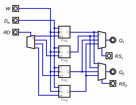
- W: write the data on the data line to the selected destination register.
- Review how to store data in a register.
- What if I wanted to could I use a ROM to store the control/data to save data into this register file.
- Idea:
- 0x101AA would be
- 1 0000 0001 1010 1010
- The data is 1010
- The data to bus is 1, so the data would go from the ROM to the BUS
- The RS1 to BUS is 0, so no data from the RF to the bus (this is good, no bus contention)
- RS1, RS2 and RD are all 0, so the 0 register is elected
- Write is 1, so we will be writing to RD, or register 0
- Add a ROM to store my program.
- This will need to be 17 bits wide for the above control bits.
- And Let's make it 8 bits tall, (for an 8 operation program)
- How would I build a bus?
- Just an 8 bit wire with an output.
- I will hook the bottom 8 bits from the ROM to this
- But I need to make sure that only one source was putting data on the bus
- So ROM 0-7 needs to go through an 8 bit tristate device
- Which is controlled by the ROM to BUS line
- And the rs1 needs to go through an 8 bit tristate device
- Which is controlled by the RS1 to Bus line.
- I had a timing issue, so I wanted to make sure that these two were never on at the same time.
- I added a delay circuit to the RS1 to Bus line.
- I still have an occasional race condition here, but we will ignore that for now.
- One other issue is the clock
- Remember, data needs to stabilize before we put it into the register.
- So I added a clock, that I and with the Write bit when I am ready to store the data.
-
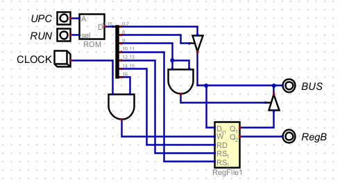
- simpleCPU.dig, but you also need RegFile1.dig.
- I evenually wrote this program
0x101AA
0x141BB
0x181CC
0x1C1DD
0x00E00
0x01200
0x02600
0x03A00
Bits Meaning 0-7 Data 8 Data To BUS 9 RS1 To BUS 11-12 RS2 13-14 RS1 15-16 RD 17 Write - 0x101AA would be